Hardware Engineer & Researcher

Sudipta Romen Biswas

Building next-generation optical sensing systems at Meta. PhD in Electrical Engineering with expertise in 2D materials, nanophotonics, and computational device modeling.

Hardware Engineer @ Meta · PhD, University of Minnesota · 457+ Citations

Sudipta Romen Biswas

About Me

Bridging academic research and industry innovation in optical systems and semiconductor devices.

I'm a Hardware Engineer at Meta, where I work on image sensor validation for AR/VR devices. My work spans the full lifecycle from design validation to production testing, ensuring world-class image quality and sensor performance.

Previously, I was an Optical Sensing Hardware Engineer at Apple focused on ambient light sensor test and validation, and contributed to LED innovation at Lumileds, bringing deep expertise in photonics and semiconductor physics to cutting-edge product development. At Lumileds, I co-invented patents spanning microlens arrays, air-spaced optics, pcLED structures, and metalens-based optical designs.

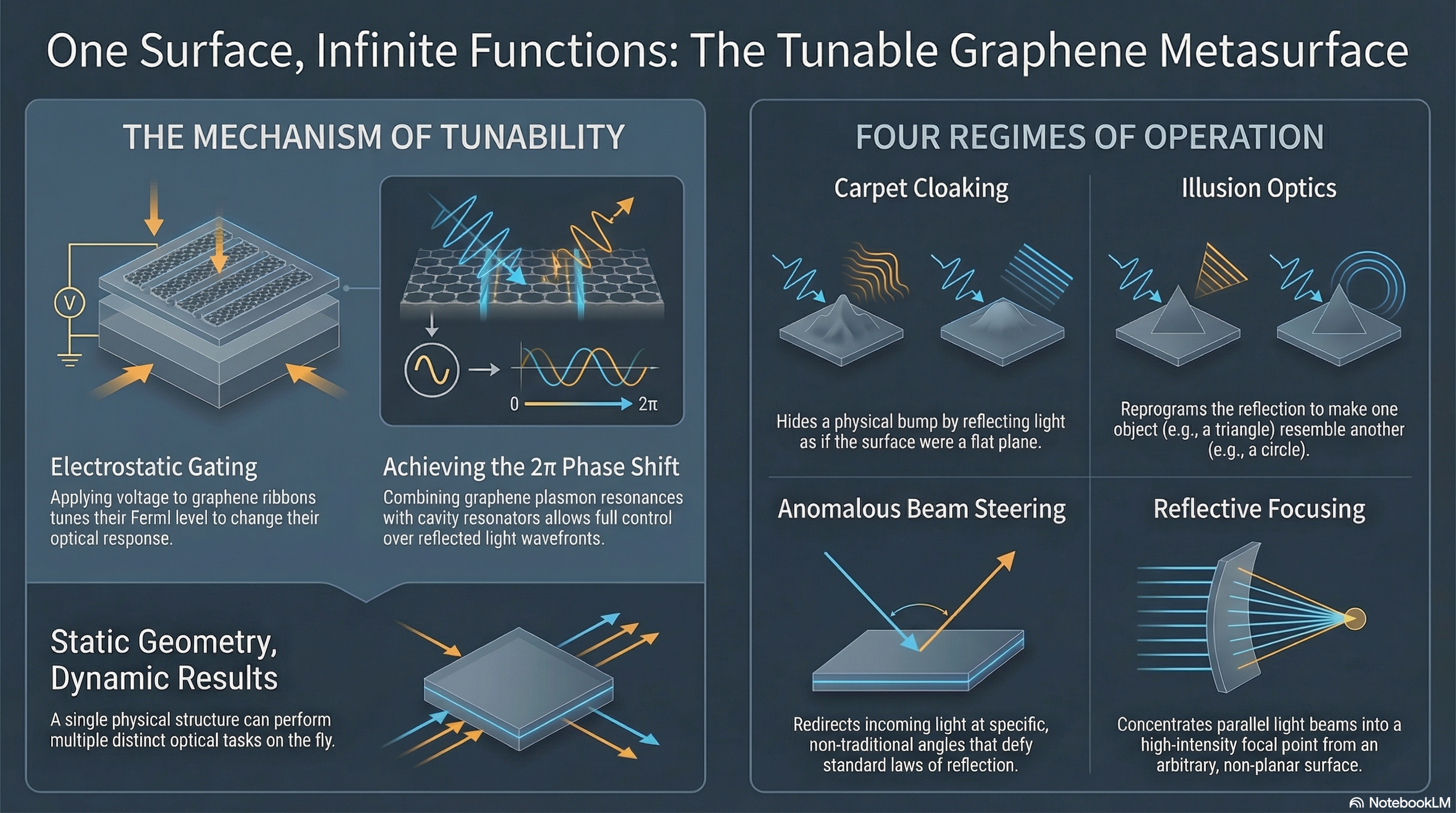
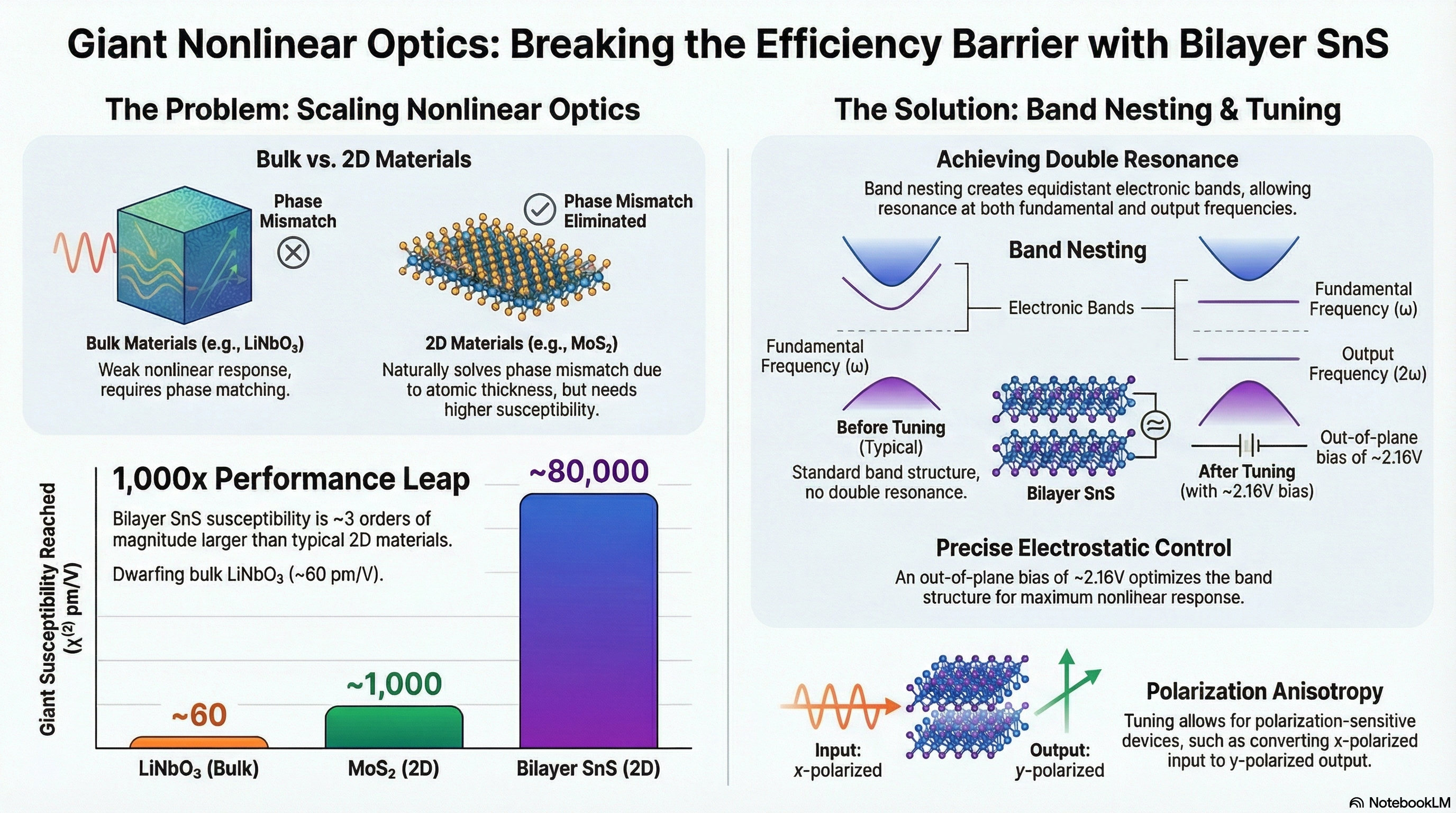
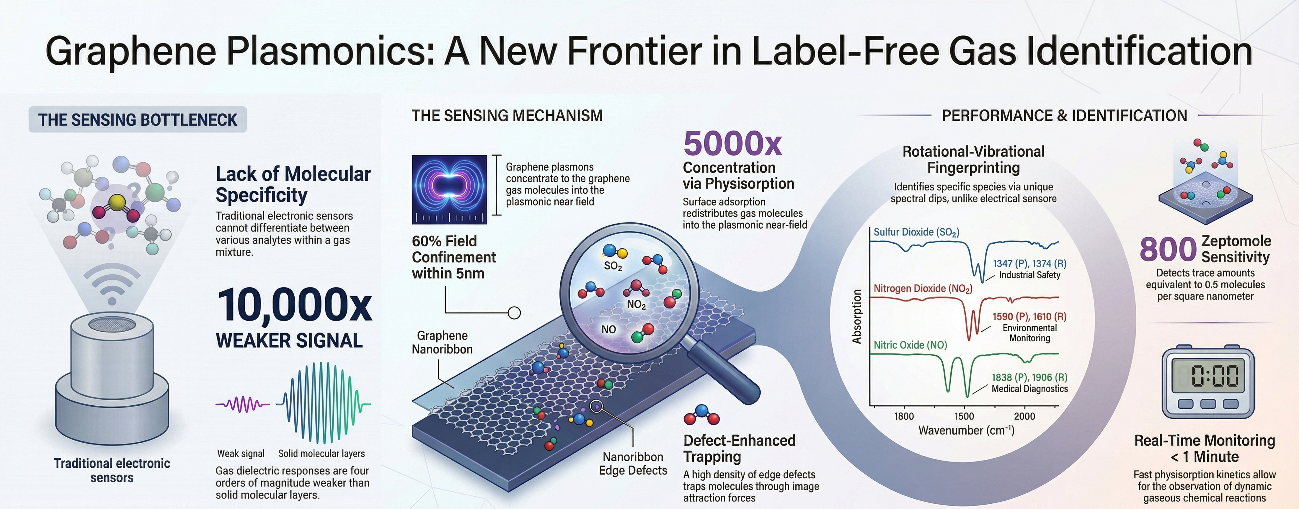
I hold a PhD in Electrical Engineering from the University of Minnesota, where I worked under Prof. Tony Low on theoretical and computational studies of two-dimensional materials and nanophotonic devices. My research has been published in top journals including Nature Communications and Physical Review, with over 457 citations.

I received my BSc from Bangladesh University of Engineering and Technology (BUET) and was awarded the prestigious 3M Science and Technology Doctoral Fellowship during my graduate studies.

When I'm not working on sensors or simulations, you'll find me playing tennis, hiking trails, or experimenting with ukulele and violin.

Work Portfolio

Post-graduate industry experience spanning optical sensors, image sensors, and LED technology at leading technology companies.

R&D Intern (2018, 2019)

Completed two summer internships at 3M's research division, contributing to materials science and device innovation projects. Work resulted in a patent application for drone-hosted construction defect remediation technology.

Materials R&D · Device Innovation · 3M Science & Technology Fellowship

Application Drone-hosted construction defect remediation US20240189850A1

Research

My PhD research at the University of Minnesota focused on theoretical and computational studies of two-dimensional materials and nanophotonic devices, supervised by Prof. Tony Low.

Graphene Metasurfaces Tunable Nonlinear Optics Plasmon-based Gas Sensing 2D Materials Computational Electromagnetics

Tunable Graphene Metasurfaces

My work in graphene metasurfaces focused on electrically reconfigurable platforms that can tune phase and amplitude in real time for beam manipulation. I developed modeling and design workflows to link gate bias, surface response, and far-field control in one framework. This project established practical directions for active, multifunctional metasurface hardware.

Tunable graphene metasurface: mechanism of tunability and four regimes of operation

Tunable Graphene Metasurface Reflectarray

An electrically controlled graphene reflectarray design that demonstrates dynamic beam steering and wavefront shaping through programmable phase modulation.

143 citations · Physical Review Applied

View Publication

Tunable Nonlinear Optics in 2D Materials

This project explored how band-structure engineering in layered materials can amplify and tune nonlinear optical behavior. I studied resonance-driven mechanisms that connect electronic transitions to strong frequency-conversion response. The outcome was a clearer path for designing compact nonlinear photonic components using 2D materials.

Giant nonlinear optics via band nesting in bilayer SnS

Double Resonant Second Harmonic Generation via Band Nesting

This paper shows that band nesting under resonant excitation can strongly enhance second-harmonic generation in layered 2D systems.

Physical Review B · 5 citations

View Publication

Tunable Hyperbolicity and Nonlinear Response in 2D Materials

This work links tunable electronic structure to anisotropic hyperbolic dispersion and enhanced nonlinear optical response in two-dimensional materials.

View Publication

Plasmon-based Gas Sensing

This work investigated graphene plasmonics for molecular sensing by matching infrared resonances to chemical fingerprints. The research emphasized label-free detection strategies with high sensitivity enabled by strong near-field confinement. These studies demonstrated how tunable plasmonic platforms can support compact and selective gas sensing.

Graphene plasmonics for label-free gas identification: sensing mechanism and performance

Gas Identification with Graphene Plasmons

A label-free sensing approach that uses graphene plasmon resonances to detect and identify gases through their infrared fingerprint signatures.

257 citations · Nature Communications

View Publication

Plasmonic Gas Sensing with Graphene Nanoribbons

This study shows how localized nanoribbon plasmons increase light-matter interaction to improve compact gas sensor sensitivity and selectivity.

44 citations

View Publication

Undergraduate Research: III-V Transistor Modeling

During my undergraduate research at BUET, I modeled III-V quantum-well transistor behavior using quantum ballistic simulation methods. I analyzed transport and capacitance-voltage trends to evaluate scaling potential for high-performance logic devices. This work built my early foundation in device physics and computational modeling.

Quantum Ballistic Modeling of InGaAs/InAs Quantum-Well MOSFETs

A quantum ballistic modeling study of InGaAs/InAs quantum-well MOSFETs that characterizes transport and C-V behavior for next-generation scaling.

View Publication View Publication

Certifications

Selected technical certifications from my resume that complement my work in optics, sensing, and photonics.

Optical Engineering and Optical Instrument Design

UC Irvine Division of Continuing Education certification, currently ongoing. Courses completed so far:

  • Introduction to Lens Design — Fundamentals of optical design using ray-tracing software, with emphasis on recognizing and correcting optical aberrations.
  • Optical Systems Engineering — Systems engineering applied to optical, IR, and laser systems; covers requirements analysis, error budgets, and first-order radiometric modeling.
  • Advanced Lens Design — Higher-order aberration theory and design principles including bending, symmetry, stop shift, and lens splitting applied to complex optical systems.
  • Introduction to Fiber Optics — Analysis and design of fiber optic links covering fiber types, light propagation, and end-to-end system performance.

UC Irvine DCE · Ongoing

Silicon Photonics Design, Fabrication and Data Analysis

UBC's Phot1x on edX — the first online course covering the full design-fabricate-test cycle for silicon photonic ICs. I designed 7 imbalanced Mach-Zehnder interferometer (MZI) circuits using the SiEPIC PDK in KLayout, simulated mode profiles and circuit transfer functions in Lumerical MODE and Interconnect, and submitted the layout for fabrication via the Applied Nanotools NanoSOI EBeam process (220 nm SOI, October 2025 run). Post-fabrication, I extracted free spectral range and group index from measured spectra through curve-fitting, validated against simulation, and performed corner analysis to characterize group index variation with fabrication tolerances.

edX · UBCx Phot1x · University of British Columbia

View Design Report

Let's Connect

I'm always interested in discussing optical systems, nanophotonics, or potential collaborations. Feel free to reach out through any of the channels below.